CMOS-Compatible and Scalable Electrochemical Synaptic Transistor Arrays for Deep-Learning Accelerator
Authors: Jinsong Cui, Fufei An, Jiangchao Qian, Yuxuan Wu, Luke L. Sloan, Saran Pidaparthy, Jian-Min Zuo, Qing Cao*
Highlighted by ScienceDaily, Science Magazine, TechXplore, Today Headline, Electronics for You, News8Plus, Semiconductor Engineering, and more
Background
In-memory-computing architectures based on memristive crossbar-arrays can enhance the computing efficiency for deep-learning with massive parallelism. However, to fulfill their potential, the core memory devices must be capable of providing high-speed and symmetric analog programing with small variability, compatible with silicon technology, and scalable into nanometer-size footprint. We present an electrochemical synaptic transistor, built with CMOS-compatible metal oxides and operating by shuffling protons within a symmetric gate stack, to meet all these stringent requirements. It can be monolithically integrated with silicon transistors to form pseudo-crossbar arrays where parallel, precise, and symmetric programming of the channel conductance can be executed with gate-voltage pulses. High-speed programing with frequency approaching megahertz, endurance above 100 million read-write pulses, and device dimensions down to 150×150 nm2 have all been realized.
Electrochemical Random-Access Memory (ECRAM)
Considering these challenges, 60 years after their first implementation in constructing artificial neural networks in 1960s, electrochemical synaptic transistors have resurfaced as a candidate to realize deep-learning accelerators based on the in-memory-computing architecture. Their channel conductance can be precisely modulated by the electrochemical intercalation reactions controlled with the bias applied on the separate gate terminal, which provides multistate analog programing with high symmetry and low variability. However, the electrolytes employed in most existing ECRAM devices are either liquid or organic polymers, which are very difficult, if not impossible, to be incorporated into scaled memory cells with the long-term stability and reliability required for electronic applications, and they are only functional in a controlled environment. There are some all-solid-state inorganic ECRAM designs, but they operate based on the intercalation of either lithium ions, which are not compatible with silicon-CMOS as lithium ions can readily diffuse across various oxides into the silicon lattice and dramatically change the silicon carrier concentration as shallow interstitial dopants, or oxygen, whose sluggish motion limits the device programing speed above several milliseconds.
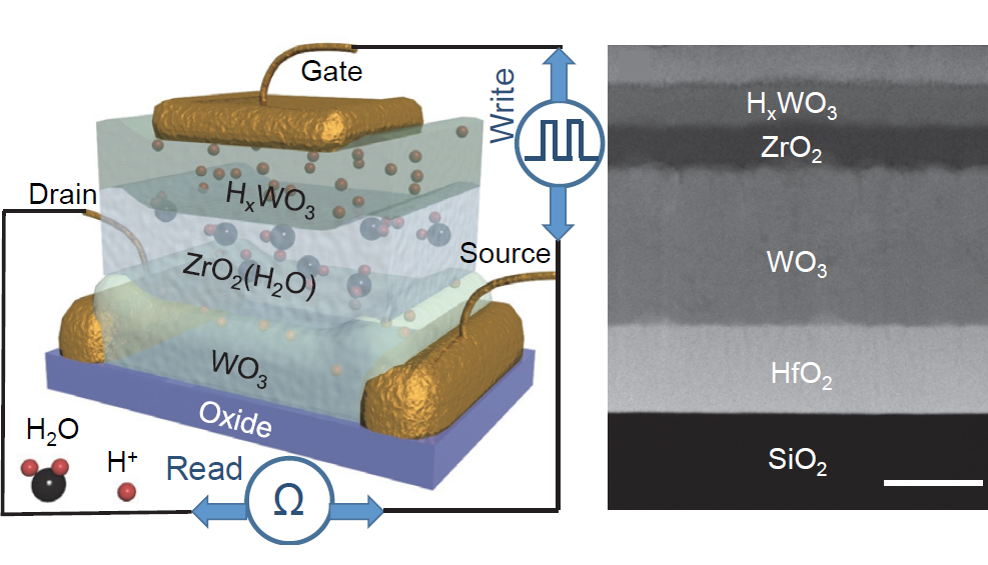
Here we present an all-solid-state inorganic ECRAM prototype operating based on the reversible insertion of protons into a WO3 channel from hydrogenated ZrO2 electrolyte and HxWO3 gate. These devices can simultaneously meet requirements on the programing symmetry and variability, device endurance, CMOS-compatibility, and device scalability for the ideal memristive devices for constructing deep-learning accelerators. They exhibit highly symmetric and reproducible programing under gate-voltage pulses with endurance above 100 million read-write operations. Both WO3 and ZrO2 are compatible with the silicon-CMOS technology and associated microfabrication techniques, allowing the unprecedented scaling of ECRAM dimensions down to 150×150 nm2. With amorphous HfO2 as both the interlayer dielectric and proton-diffusion barrier, these ECRAMs can be fabricated above silicon circuits without affecting the performance of the underlying logic transistors. ECRAM pseudo-crossbar arrays addressed with silicon selector transistors were then realized for the first time to demonstrate successfully parallel operations and monolithic integration. The small radius of the proton intercalant enables fast ionic dynamics for high-speed write-read programing with frequency approaching one megahertz. The non-volatile conductance of these CMOS-compatible protonic ECRAMs can be tuned over a wide range from nano to micro-siemens, enabling the construction of large-size arrays with optimum power and performance. These results have established this ECRAM prototype as a prominent candidate for the core memory element in the next-generation analog deep-learning accelerators, with their current level of performance and non-idealities already sufficient to support training accuracy comparable to that of digital accelerators based on static random-access memory (SRAM), but under drastically reduced chip-area cost and energy consumption.
