Solution-processable ordered defect compound semiconductors for high-performance electronics
Authors: Hsien-Nung Wang1, Fufei An1, Cindy Y.Wong, Kaijun Yin, Jiangnan Liu, Yihan Wang, Jian-Min Zuo, André Schleife and Qing Cao*
Feature Article of Science Advances, Highlighted by Nature Electronics, MSN, Science Daily, TechXplore, Semiconductor Engineering, Nanowerk, Display Daily, ASM International, and more
Background
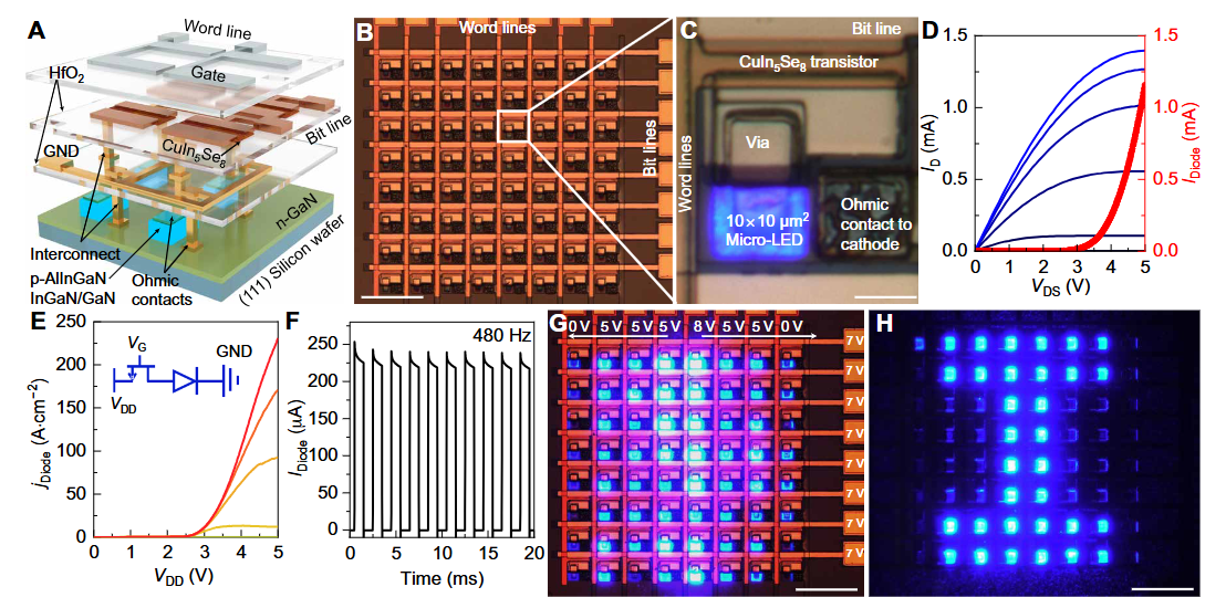
Solution-processable semiconductors allow scalable and cost-effective manufacturing of solid- state electronic devices. Nevertheless, the performance of transistors built on various semiconductors grown from solution, including silicon, metal oxides, metal chalcogenides, colloidal quantum dots, perovskites, one-dimensional (1D) or 2D nanomaterials, and organic semiconductors, is severely limited by the prevalence of material structural defects, which are formed from corresponding solution precursors in a kinetically controlled deposition process with limited thermal budget. It precludes their adoption in emerging applications, which need not only low-cost and high-throughput fabrication of electronics but also high performance, e.g., high-speed logic circuits for ubiquitous edge computing and high- resolution display backplanes driving miniaturized nitride light-emitting diodes (microLEDs)
Cu-In-Se defect compound semiconductors
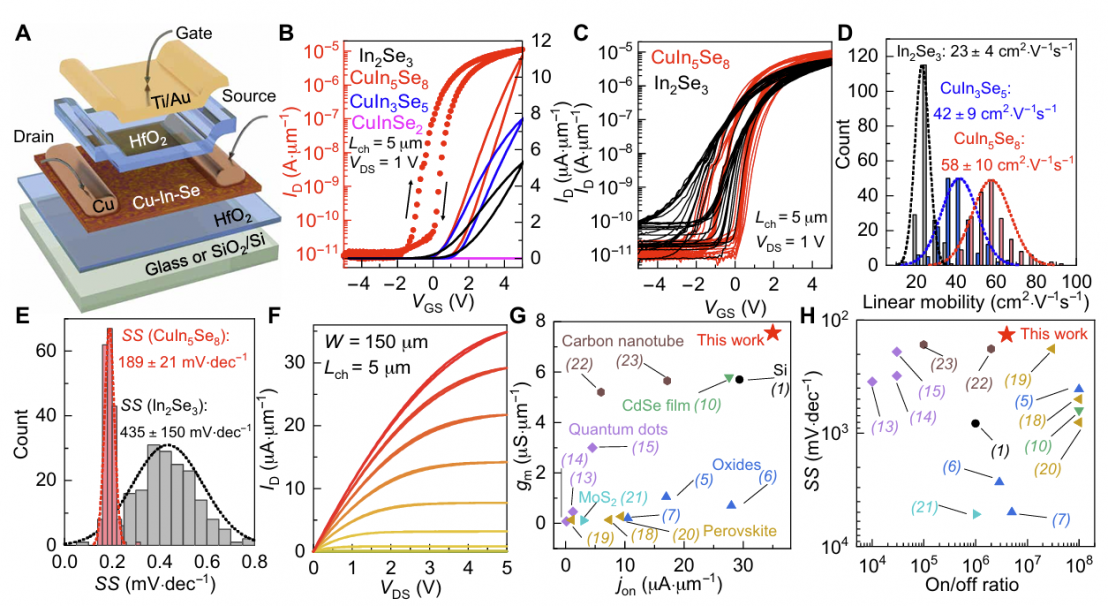
The ternary Cu-In-Se compounds along a composition tie-line connecting Cu2Se and In2Se3 form a family of semiconductors. In addition to CuInSe2 and In2Se3, which have drawn broad interest for their use in solar cells and transistors, there are another two single- phase regions corresponding to indium-rich stoichiometries of CuIn3Se5 and CuIn5Se8. Here we show that ordered defect compound semiconductor CuIn5Se8, which forms regular defect complexes with defect-pair compensation, can simultaneously achieve high performance and solution processability. CuIn5Se8 transistors exhibit defect-tolerant, band-like transport supplying an output current above 35 microamperes per micrometer, with a large on/off ratio greater than 106, a small subthreshold swing of 189 ± 21 millivolts per decade, and a high field-effect mobility of 58 ± 10 square centimeters per volt per second, with excellent uniformity and stability, superior to devices built on its less defective parent compound CuInSe2, analogous binary compound In2Se3, and other solution- deposited semiconductors. They can be monolithically integrated with carbon nanotube transistors to form high- speed and low-voltage three-dimensional complementary logic circuits and with micro-light-emitting diodes to realize high-resolution displays.

